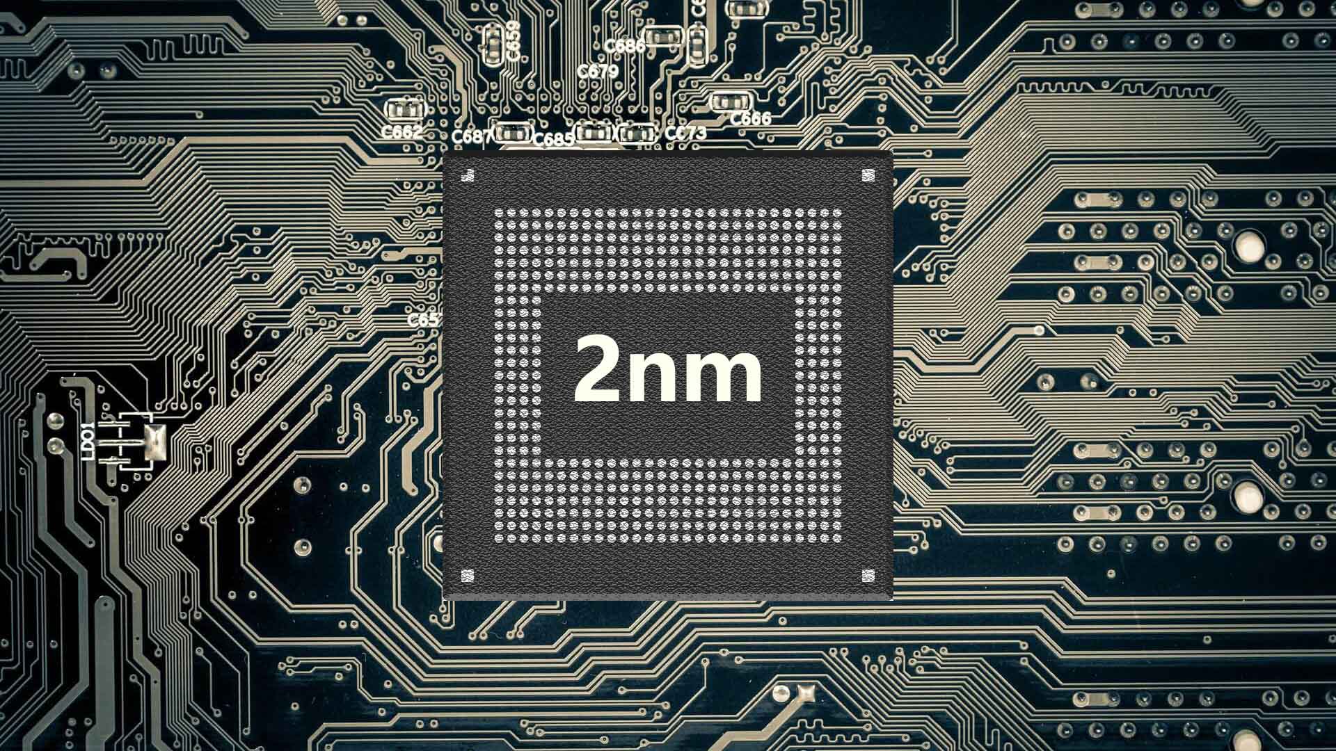
Samsung has finally lifted the curtain on its long teased 2 nanometer gate all around manufacturing node, putting real numbers on performance, power and yield instead of vague promises. The company now claims up to a 5 percent performance uplift and up to 8 percent better power efficiency compared with its first generation 3 nanometer GAA process, while keeping about a 5 percent area reduction. 
Those may not be the jaw dropping gains some enthusiasts imagined, but they mark a more realistic snapshot of where the technology stands today.
Until now, Samsung had mostly talked about 2 nanometer in terms of roadmaps and mass production milestones. Wafers were said to be in volume production, yet there was little clarity on what customers or consumers would actually gain. With this disclosure, the picture sharpens. The first major chip built on the node is expected to be the Exynos 2600, Samsung’s next flagship mobile platform that will power future Galaxy smartphones and tablets, and likely serve as a showcase for the new process.
On paper the jump from 3 nanometer to 2 nanometer looks modest, especially when stacked against earlier internal targets. Previous guidance suggested that Samsung was aiming for up to 12 percent higher performance and up to 25 percent better power efficiency at the same complexity, plus the same 5 percent area reduction. The new official figures of 5 percent and 8 percent therefore represent a sobering revision, hinting at the brutal difficulty of extracting large gains from cutting edge geometry shrinks in the post FinFET era.
Even so, an 8 percent power saving can be extremely valuable in real products. For battery limited devices like smartphones, laptops and wearables, shaving off nearly a tenth of power at the same performance level can translate into cooler operation, longer battery life or extra headroom for bursts of performance. Chip designers can choose how to spend that efficiency budget, whether on higher clocks, more cores or simply on hitting the same targets at a lower cost and voltage.
Behind the performance curves, yields tell an equally important story about the maturity of Samsung foundry. Not long ago, reports suggested that usable 2 nanometer yields hovered around 30 percent, a level that makes large scale production painfully expensive. The latest numbers in the 50 to 60 percent range do not yet match the comfortable territory of a fully mature node, but they are a huge step forward, potentially halving the number of discarded dies per wafer and bringing costs much closer to commercially viable levels.
These yield gains unlock new business. According to industry reports, Samsung had been limiting Exynos 2600 output to around fifteen thousand wafers per month while it tuned the line. With yields rising, the company can finally ramp. Two of the world’s biggest cryptocurrency mining equipment vendors, MicroBT and Canaan, have already booked 2 nanometer capacity that together equals roughly ten percent of Samsung’s total production, a strong vote of confidence from clients who live or die by efficiency per watt.
On top of that, Samsung has reportedly signed a multibillion dollar deal with Tesla, making the 2 nanometer node a key piece of the electric car maker’s future self driving and AI silicon. Automotive chips demand long lifecycles, reliability and a tight power envelope, so securing a design win there suggests that partners trust Samsung’s roadmap. The company’s foundry share still sits at about 7.3 percent versus TSMC’s commanding 70.2 percent, but anchor customers like Tesla give Samsung valuable experience and branding at the high end.
Inside Samsung, the stakes are even higher. Management has set an ambitious goal of returning the semiconductor division to solid profitability by 2027, and 2 nanometer is clearly positioned as the foundation for that turnaround. Success will depend not only on transistor specs, but also on predictable yields, competitive pricing and the ability to attract more designers away from rival fabs. Each wafer that ships, whether bound for a Galaxy phone, a mining farm or an electric vehicle, helps to chip away at the perception gap with the market leader.
Among enthusiasts, reactions to the new figures are mixed. Some fans expected dramatic double digit performance leaps and greeted the five percent number with a shrug or a meme. Others point out that the real headline is not raw speed, but the combination of efficiency, yields and customer momentum. After several rocky years, every incremental gain suggests that Samsung is slowly but surely stabilising its cutting edge process technology. The 2 nanometer era will not be defined by a single eye catching percentage, but by whether Samsung can consistently deliver chips that are fast, efficient and actually available in volume.
2 comments
As a miner all I care about is joules per hash, if 2nm GAA gives even a few percent better efficiency I am in, fans already sound like jet engines 😅
If Tesla is trusting Samsung with self driving chips then yeah, Samsung foundry might actually be back this time