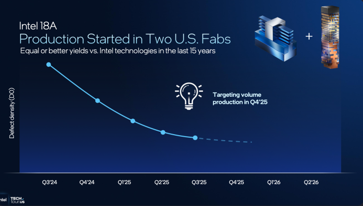
Intel’s 18A node has officially crossed a major milestone, marking one of the most decisive moments in the company’s comeback strategy. During its latest Tech Tour, Intel revealed that the 18A process technology has reached a record-low defect density – an essential measure of manufacturing maturity and readiness for both internal and external customers. In simple terms, this means the process has never been cleaner, more stable, or more efficient at producing usable chips, paving the way for mass production scheduled for the fourth quarter.
This achievement is not just a technical win; it’s a strategic one. 
Intel Foundry Services (IFS) is under the microscope like never before – watched by industry partners, investors, and even governments who view chip manufacturing as a matter of national interest. The 18A process, built to power everything from high-performance computing (HPC) chips to advanced consumer processors, needs to prove that Intel can once again compete head-to-head with the likes of TSMC and Samsung. With defect density at an all-time low, the company is signaling to the world that its manufacturing engine is humming again.
For context, defect density refers to the number of physical flaws per unit area on a silicon wafer. These defects can range from microscopic particles that disrupt transistor patterns to alignment errors that render sections of a chip unusable. The lower the defect density, the higher the yield – meaning more working chips per wafer, which directly translates into lower costs and greater scalability. Earlier reports speculated that Intel’s 18A yields were hovering around 10%, a figure that would be catastrophic for mass production. But according to Intel’s latest data, those rumors are now outdated and far from the current reality.
Lower defect rates are particularly crucial for larger die designs, such as GPUs or server chips, where even minor flaws can ruin an entire product. With the 18A node performing better than ever, Intel is positioning itself to target not only its own internal CPU roadmap but also external clients looking for an alternative to TSMC’s upcoming N2 or Samsung’s SF2 processes. These developments could mark Intel’s long-awaited return as a true foundry competitor.
Of course, defect density doesn’t tell the whole story. Other parameters – such as process margins, mask alignment accuracy, and parametric failures – still play vital roles in overall yield. But hitting this milestone is like clearing the biggest hurdle in a marathon. If Intel maintains this trajectory, it could establish 18A as a new standard for performance and reliability in advanced node manufacturing.
It’s worth noting that this momentum also sets the stage for Intel’s next major steps: RibbonFET transistors and PowerVia backside power delivery, both expected to debut with 18A. These technologies promise to further boost efficiency and performance density, strengthening Intel’s competitive edge. For now, though, the record-low defect density is the clearest sign yet that the company’s ambitious roadmap is finally paying off.
Whether this resurgence will be enough to regain market dominance remains to be seen. But one thing is certain – Intel has reentered the race with something it hasn’t had in years: real, measurable progress.
2 comments
Lisa loves her chiplets, Intel tryna play catch up again
bro the chart could be 95% to 90% who even knows lol