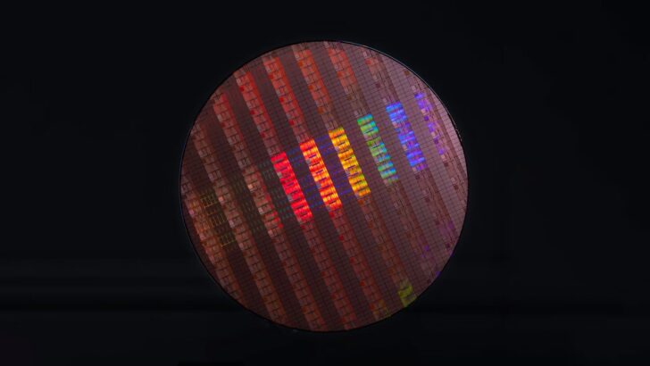
Intel’s upcoming 14A chip is already outperforming expectations, and in a surprising twist, it has reportedly surpassed the 18A node in both performance and yield – almost a year before its official debut. 
According to Intel CFO David Zinsner, the next-generation process is off to a phenomenal start, suggesting that Intel’s ambitious roadmap might finally be gaining real traction after years of delays and internal restructuring.
For context, the Intel 18A process was introduced as a symbol of the company’s comeback story. Built with RibbonFET transistors and advanced PowerVia technology, it promised massive gains in power efficiency and transistor density. Yet, the 14A node seems poised to become the true turning point. Unlike 18A, which was primarily used for Intel’s internal product lines such as Panther Lake, the 14A process is designed for external customers – the foundation of Intel’s dream to become a global foundry player capable of competing head-on with TSMC and Samsung.
In Zinsner’s words, “On 14A, we’re off to a great start. If you look at 14A in terms of its maturity relative to 18A at the same point, we’re better in terms of performance and yield.” That’s a striking statement, considering the 14A process is still nearly a year away from risk production. Intel is already engaging potential clients in early sampling phases, sharing progress updates, and incorporating customer feedback directly into development – a strategy aimed at building trust and ensuring that early adopters feel confident in committing to the process once it goes into mass production.
The 14A node is expected to bring major breakthroughs, especially with the introduction of High-NA EUV lithography and second-generation RibbonFET transistors. These technologies should push Intel’s transistor density and performance metrics even further, while simultaneously improving energy efficiency – a critical factor as chips become more complex and power-hungry. This could allow Intel to finally close the gap with, or potentially surpass, TSMC’s N2P process, which remains the current industry benchmark.
However, challenges remain. Integrating High-NA EUV is a massive technical leap, one that even TSMC has been cautious about. While Intel is eager to take advantage of the next-gen lithography tools, early yields may prove volatile. Still, this aggressive move could pay off – if Intel manages to stabilize production before its competitors transition, it might regain the technological leadership it lost during the 10nm struggles of the last decade.
Financially, the success of 14A is pivotal. The foundry market thrives on reliability, and a high-performing, high-yield node could finally make Intel’s Foundry Services division a serious contender for major clients – including AI and data center chipmakers who currently rely on TSMC. Intel aims to begin full-scale 14A production by the end of 2026, giving it just enough time to refine the process and prove that this isn’t just another overhyped milestone, but the start of a genuine comeback.
In short, while skeptics continue to doubt Intel’s consistency, the early signs from 14A hint at something different – a company that’s learning from its mistakes and betting big on regaining its place at the top of the semiconductor world. The next two years will show whether this bold bet pays off, or if it’s just another chapter in Intel’s long road of promises and delays.
2 comments
maybe they finally catching up to amd 9800x3d from 2 yrs ago lmao but at twice the watts 🤡
14A soon bois!!! maybe this time it’s actually real 😅