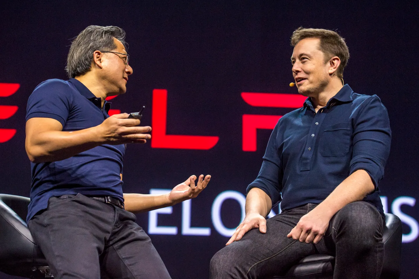
NVIDIA’s Jensen Huang has a message for anyone who thinks building a cutting-edge semiconductor foundry is just a matter of money and blueprints: it isn’t. 
Responding to Elon Musk’s idea of creating a gigantic in-house fab – capable, in Musk’s telling, of ultimately turning out around a million custom AI chips per month – Huang stressed in Taiwan that what Taiwan Semiconductor Manufacturing Company (TSMC) does every day is not simply manufacturing; it’s an intricate blend of science, engineering, logistics, and hard-earned craft.
The context matters. Tesla’s appetite for specialized silicon is exploding as it pursues full self-driving, robotaxi ambitions, and humanoid robotics. Musk’s pitch is that today’s capacity from TSMC, Samsung, and possibly Intel may be too tight or too expensive to secure the long-term volumes Tesla envisions. Hence the notion of a so-called “TeraFab.”
Why ‘just build a fab’ dramatically understates the challenge
At advanced nodes, success hinges on yield – how many defect-free chips you get per wafer – and on the ability to improve that yield week after week. That means armies of process engineers, materials scientists, lithography specialists, and metrology experts iterating constantly. It also means a web of suppliers delivering ultra-pure gases, photoresists, wafers, and precision components at staggering reliability levels. Even veteran players stumble; Intel’s multiyear struggles to regain leadership show how unforgiving the learning curve can be.
- Capital intensity: a modern leading-edge fab easily soars into the tens of billions of dollars before the first high-volume wafer ships – then demands ongoing reinvestment every node.
- Tool bottlenecks: extreme ultraviolet (EUV) scanners from ASML arrive in limited quantities, and the queue is long. Without the tools, even limitless cash can’t buy time.
- Yield learning: ramping from pilot to profitable mass-production takes years. Each new process step introduces hidden variables that must be tamed.
- Risk management: a single out-of-spec chemical lot can jeopardize weeks of output. The operating discipline is as critical as the blueprint.
Huang’s point isn’t that ambition is futile. It’s that TSMC’s advantage is cumulative: decades of process learning, a culture optimized for foundry work, and a customer roster that keeps its lines full and its feedback loop fast. NVIDIA’s own AI surge rides on that ecosystem; TSMC is the beating heart of Team Green’s data-center roadmap.
Could Musk shortcut the timeline?
Some industry voices argue the real choke point isn’t TSMC per se but EUV tool supply. If ASML can only ship so many scanners, any newcomer spends years waiting in line. Others suggest a faster route might be to buy an existing foundry, co-invest with a partner, or pre-pay for mountains of capacity – tactics that have worked for hyperscalers and chip designers when cycles run hot. A GlobalFoundries acquisition would bring facilities and talent, but not the latest node leadership; catching up to 3 nm, let alone 2 nm and beyond, is its own marathon.
There’s also a market dimension. If Tesla truly needed a million AI accelerators monthly, that tidal wave would reshape pricing, supply chains, and power infrastructure. Incumbents would respond aggressively – Samsung Foundry and Intel Foundry Services are hunting for marquee anchor customers – and governments would be eager to subsidize jobs and resilience. Yet even with subsidies, the yield ramp is non-negotiable.
The case for audacity – tempered by reality
Musk has a track record of turning scoffs into shipping products – reusable rockets, mass-market EVs, and global satellite internet. That history is why some technologists welcome his attempt to diversify the foundry game, even if it takes a decade to truly bear fruit. Still, rockets and fabs differ in crucial ways: launch cadence rewards fast iteration; wafer fabs punish it with ruinous scrap and microscopic tolerances.
Bottom line: Building a leading-edge fab is possible with enough capital, patience, and world-class talent – but matching TSMC’s consistency at scale is the hardest part.
What seems most likely
- Partnership first: Tesla continues to lean on TSMC (and perhaps Samsung/Intel) while negotiating multi-year, prepaid capacity with tighter design–manufacturing co-optimization.
- Selective vertical integration: a specialized back-end or packaging facility (e.g., advanced 2.5D/3D integration) could appear before a full front-end fab, improving performance without reinventing all of lithography.
- Long-horizon fab bet: if a TeraFab proceeds, expect timelines measured in many years, capex in the hundreds of billions over iterations, and an early focus on a narrow set of Tesla-specific chips to simplify yield learning.
Huang’s caution and Musk’s ambition aren’t opposites; they’re the two forces that shape semiconductor progress. The former reminds us why TSMC is singular. The latter ensures the industry keeps pushing at what once looked impossible.