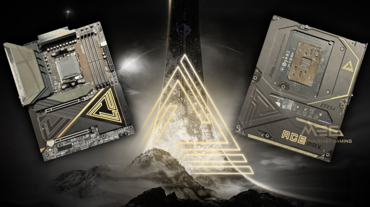
MSI MEG X870E ACE Max: an enthusiast board built for AMD’s next 3D V-Cache wave
MSI’s ACE badge returns to the AM5 arena with the MEG X870E ACE Max, a flagship motherboard that pairs deep overclocking tools with creature comforts and forward-looking I/O. First teased alongside the Z890 family and shown again during Computex 2025, this X870E refresh is clearly engineered with AMD’s incoming Ryzen 3D V-Cache refresh in mind – right down to an expanded 64 MB BIOS and a discrete clock generator that targets higher performance ceilings.
Power delivery and platform backbone
At the heart of the board is a robust 18+2+1 (110 A) VRM architecture fed by dual 8-pin EPS connectors. The phase count and current rating signal headroom for heavy all-core loads and sustained boost behavior, which is precisely what top-end Ryzen parts – especially dual-CCD 3D V-Cache SKUs – tend to demand. MSI pairs the stages with a dense, wavy-fin VRM heatsink array linked by a direct-touch cross heat pipe, plus 9 W/mK thermal pads to keep transistor and chokes temperatures in check during long render or compile runs.
Memory and the overclocker’s toolkit
The X870E ACE Max carries four DDR5 DIMM slots with support for high memory frequencies and tight subtimings, but the real headline for tweakers is MSI’s OC Engine – a dedicated clock generator on the board. MSI touts up to ~15% uplift in some workloads by decoupling bclk from other domains. Complementing it is the Direct OC Jumper, a hardware pathway for real-time BCLK tuning that makes iterative stability testing less of a reboot marathon. As with any bclk-based push, expect your mileage to depend on the specific CPU, IMC quality, and cooling, but the tools here are clearly deeper than on typical premium boards.
BIOS capacity ready for what’s next
MSI’s entire “MAX” line moves to a 64 MB UEFI, which sounds mundane until you realize how tight firmware budgets can get when adding microcode, AGESA updates and utility modules. The larger ROM should mean fewer tradeoffs as AMD ships new AGESA for the 3D V-Cache refresh – out-of-the-box support is the promise – and better long-term maintainability for early adopters.
Storage and PCIe layout
Fast storage is a given at this tier, but the ACE Max still overachieves: five M.2 sockets live under M.2 Shield Frozr heatsinks, with two Gen5 links for bleeding-edge SSDs. The first slot uses an EZ Magnetic M.2 Shield Frozr II – a handy, toolless magnetic heatsink – while the remaining sockets feature the EZ M.2 Clip II latch. On the graphics side, the top PCIe 5.0 x16 slot includes EZ PCIe Release so you can free a triple-slot GPU without contortions. There’s also a single 8-pin auxiliary power feed aimed at stabilizing power to the PCIe lanes during extreme setups, and the board presents dual PCIe 5.0 x16 mechanical slots for flexible add-in card layouts.
Connectivity and rear-panel I/O
Flagship connectivity is table stakes and MSI checks the boxes: 10 GbE LAN for workstations and NAS-heavy homes, Wi-Fi 7 for high-throughput wireless, and USB 40G ports for fast external SSD workflows and high-bandwidth docks. While MSI hasn’t enumerated every port in this briefing, the portfolio aligns with what creators and high-fps gamers expect from an ACE-class board in late-gen AM5.
Cooling design, build, and that ‘Illusion Lightning’ look
Beyond raw thermals, the board’s visual language is unmissable. The new Illusion Lightning treatment animates the front I/O shroud – complete with the MSI dragon – while a sweeping PCH/M.2 cover ties the lower half together. Flip it over and you’ll find a metal backplate finished in black-and-yellow accents that complement the front-side palette. The brushed and polished areas are so reflective that, during our hands-on time, you could practically see your outline in the sheen – gorgeous for clean builds, though you’ll want a microfiber nearby if fingerprints drive you up the wall.
Quality-of-life touches
The toolless M.2 system genuinely reduces build friction, particularly when swapping Gen5 drives that run hot enough to warrant frequent heatsink checks. The EZ PCIe Release tab is another small thing that becomes a big thing the first time you pull a massive GPU from a cramped case. Sprinkle in diagnostic conveniences and the OC switches, and the board reads as equal parts showpiece and serious platform for iteration.
Positioning in MSI’s AM5 stack and timing
MSI has already begun retail rollout of its X870/X870E family; we recently tested the X870E Tomahawk MAX WiFi, and broader availability is ramping. The MEG X870E ACE Max sits above those mainstream heroes, targeting builders who want the best AM5 experience today and a glide path to AMD’s next cache-stacked chips tomorrow. MSI indicates the ACE Max is expected around CES 2026, which tracks with the cadence of AMD’s rumored refresh window.
Early verdict
With a 21-phase 110 A VRM, a real clock-gen-powered OC Engine, five M.2 (two at Gen5), Wi-Fi 7, 10 GbE, and a capacious 64 MB BIOS, MSI’s MEG X870E ACE Max looks every bit the no-compromise AM5 flagship. It’s designed to be both a stable daily driver and an exploratory platform for bclk tinkerers – exactly the blend we want as Ryzen’s 3D V-Cache refresh approaches. If your next build chases top-tier gaming and creator thermals with a side of showpiece aesthetics, this ACE could be the new bullseye.
2 comments
So shiny lol, I can kinda see the photographer in the 3rd pic 😂 polishing cloth required
That OC Engine + real bclk jumper is the real deal. If it does even 5–10% on my 7800X3D, I’m sold