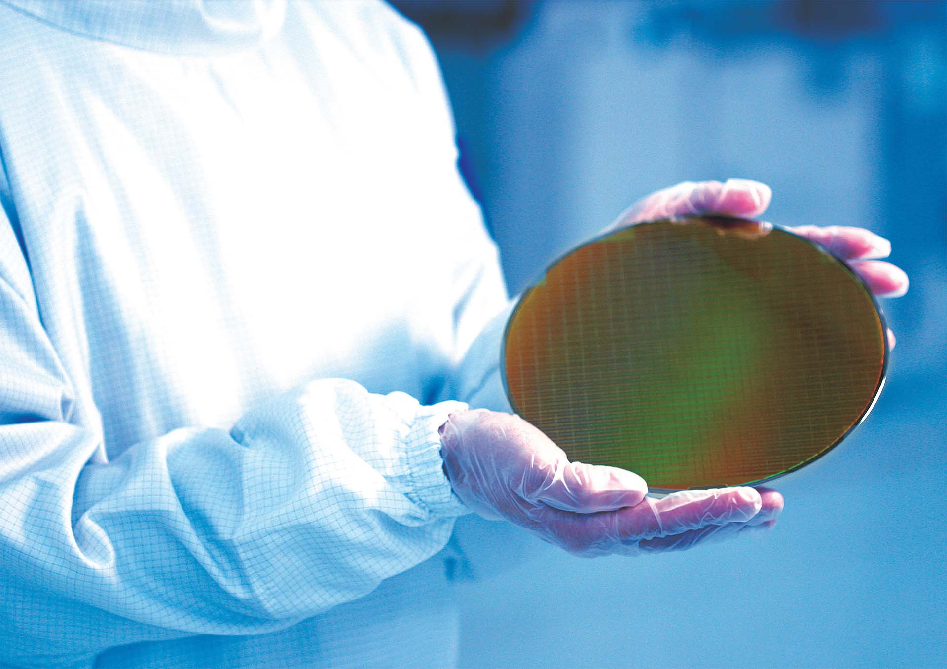
At the eighth Semiconductor Industry-Academia-Research Exchange Workshop in Seoul, Samsung Electronics Foundry Vice President Shin Jong-shin made a statement that resonated deeply across the chipmaking world: “Process miniaturization alone can now only deliver a 10–15% improvement.” That remark reflects a growing truth in the semiconductor industry – simply shrinking transistors is no longer enough. The days when every new node brought massive leaps in performance and power efficiency are over. 
To keep progress alive, the focus has shifted to smarter design collaboration and holistic engineering approaches like Design-Technology Co-Optimization (DTCO).
Samsung’s 2nm Gate-All-Around (GAA) process represents one of the company’s most advanced nodes yet, offering notable performance and power efficiency gains compared to earlier FinFET-based technologies. However, Shin emphasized that as physical scaling nears atomic limits, additional gains require integrating design and process improvements hand-in-hand. “At 7nm, about 10% of improvements came from DTCO,” he said. “We expect that share to hit 50% at 3nm and below.” This means that half of the performance uplift of future chips will depend not on smaller transistors, but on smarter engineering.
DTCO isn’t just a buzzword. It’s a strategic methodology combining circuit design, process technology, and architecture optimization to overcome the inefficiencies that appear when traditional scaling slows down. In practice, Samsung and TSMC have both formed dedicated DTCO teams to push boundaries, refining how design interacts with the manufacturing process. The Elec reports that in Samsung’s case, these teams even work with clients like Tesla to customize and reconfigure layouts to improve power and area efficiency.
Samsung’s ongoing transition from FinFET to GAA technology illustrates this philosophy. Its first 3nm iteration faced yield challenges, but the upcoming 2nm version shows significant promise. Shin explained that even a mere 1–2% improvement matters immensely at such scales: “In the world of semiconductor processing, a 1% gain can determine the chosen process node.” These incremental yet vital improvements are increasingly shaped by AI-assisted design tools. Samsung’s engineers are already using artificial intelligence to automatically create optimized cell structures that minimize area and power consumption.
Looking ahead, Samsung’s vision goes beyond DTCO. The company is expanding toward System-Process Co-Optimization (SPCO) and System-Design-Process Co-Optimization (SDTCO) – frameworks that extend optimization from transistor level to entire systems. These methods could align hardware and software design cycles to achieve leaps in energy efficiency and integration that scaling alone cannot deliver. According to reports, Samsung has completed the basic design for its second-generation 2nm process and plans to introduce an enhanced SF2P+ variant within two years. Its cautious approach, prioritizing refinement over rushing to 1.4nm, suggests that Samsung aims for maturity and stability rather than headline-grabbing announcements.
The semiconductor race has evolved from a contest of who can etch smaller transistors to who can design smarter chips. IBM predicted the end of transistor scaling over a decade ago, and now the industry is living through that reality. As AI, quantum computing, and advanced packaging become more intertwined with chipmaking, Samsung’s focus on co-optimization may define the next decade of semiconductor progress.
1 comment
DTCO feels like the only way forward, packaging tech alone won’t save anyone